
Antiferroelectric materials represent a captivating frontier in condensed matter physics, characterized by their unique electric dipole arrangements. Unlike traditional ferroelectrics, where dipoles align in a uniform direction, antiferroelectrics exhibit a fascinating property: their dipoles can perfectly cancel each other out, resulting in no net polarization. This cancellation leads to numerous applications in advanced technologies, particularly in energy storage, memory devices, and sensors. As the demand for efficient and sustainable energy solutions increases, the importance of these materials cannot be overstated. Researchers at the University of Chicago have recently taken a significant step toward unlocking the full potential of antiferroelectric materials through groundbreaking imaging methods, allowing for unprecedented insights into their electronic properties.
Challenges in Imaging Antiferroelectric Materials
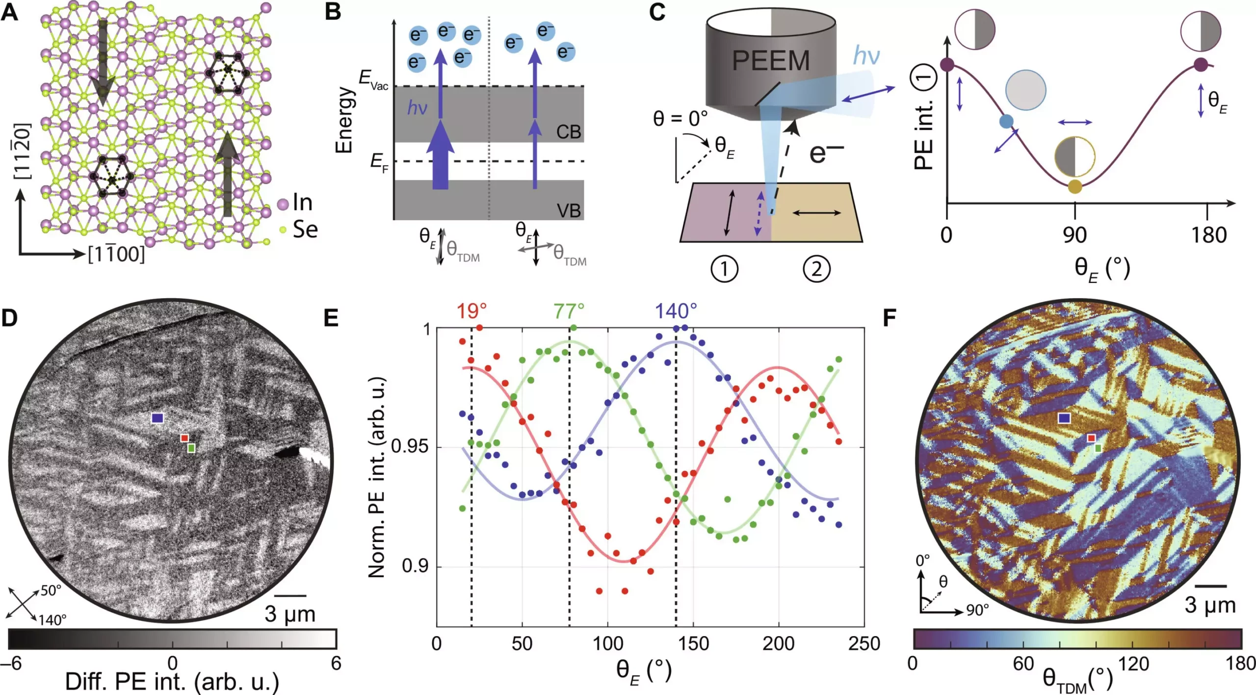
Despite the tremendous promise offered by antiferroelectric materials, researchers have faced a myriad of challenges in adequately characterizing and understanding their behavior. Traditional imaging techniques often struggled to provide the necessary resolution and contrast required to visualize crucial aspects of these materials. The inability to effectively image the unique domains within antiferroelectric substances has hindered progress and limited the modification and application of these fascinating materials. According to Sarah King, an assistant professor of chemistry and the senior author of the recent study, a significant hurdle in understanding antiferroelectric materials lies in the absence of reliable visualization techniques. “Without the means to visualize the domains, we are fundamentally limited in our ability to characterize and manipulate these materials,” she notes.
Advancing Imaging Techniques: A New Methodology
Recognizing the urgent need for enhanced imaging capabilities, King and her team have developed an innovative approach that has the potential to change the way researchers study antiferroelectric materials. Utilizing an advanced microscopy technique known as polarization-dependent photoemission electron microscopy (PPEEM), the team has successfully imaged a commonly used antiferroelectric material, indium selenide, in detail, revealing the intricate electronic properties that lie within. By combining polarized laser light with electron imaging, the researchers can virtually map the nanoscale arrangement and orientation of antiferroelectric domains, providing a complete picture of a material’s characteristics. This innovative method not only enhances resolution but also allows for real-time observation of domain switching phenomena, significantly broadening the scope for future research in the field.
Implications for Future Research and Applications
The implications of this new imaging technique are profound. Sarah King envisions a future where scientists can delve deeper into the realm of materials science, exploring previously uncharted territories within antiferroelectric and ferroelectric materials. The ability to observe domain switching dynamics opens the door to developing advanced applications in electronics and energy storage solutions. The study also sheds light on how different intrinsic properties within these materials interact to facilitate ordered states, emphasizing the importance of understanding hierarchy and order in domain formation.
Furthermore, the success of this imaging method paves the way for enhanced collaboration within the scientific community. By making it easier to visualize and modify antiferroelectric materials, researchers across various disciplines can now share findings and innovate collaboratively, driving advances in technology and sustainability. This multidisciplinary approach may yield transformative solutions to pressing global challenges, from efficient energy systems to unparalleled electronic devices.
The Role of Young Researchers in Innovation
Integral to this groundbreaking research are the talented students and postdoctoral researchers who contributed to the project. Graduate student Joseph Spellberg, alongside undergraduate student Lina Kodaimati and postdoctoral researcher Prakriti Joshi, played crucial roles in experimenting with the new imaging techniques. Their combined efforts reflect a vibrant academic environment that fosters innovation and nurtures young scientists. This collaborative approach not only enhances research quality but also propels the next generation of scientists into addressing real-world challenges, empowering them to be key players in the future of technology.
The strides made in imaging antiferroelectric materials symbolize a gateway to an era of technological excellence. As imaging techniques evolve and improve, the prospects for discovering new materials and their applications will only expand, creating exciting opportunities for future innovations. The relentless pursuit of knowledge and understanding in this arena stands as a testimony to humanity’s passion for exploration, forever igniting the spark of scientific curiosity in the quest to harness the rich potential of antiferroelectric materials.