
As the digital age progresses, the demand for computational power continues to spike, particularly in the realms of artificial intelligence, data analysis, and complex simulations. However, traditional supercomputers are now recognized for their staggering energy consumption, often equivalent to that of entire neighborhoods. In light of this, a transformative approach is evolving—embracing energy-efficient architectures inspired by the astonishing workings of the human brain through artificial neural networks.
The concept of utilizing charge density waves (CDWs)—electronic wave patterns that can manipulate the flow of electrons—emerges as a game-changer. This innovative strategy not only focuses on enhancing computational capabilities but also addresses the critical need for sustainability in modern computing frameworks. If we can leverage the principles behind these waves, we pave the way for a more energy-conscious future.
Unpacking Charge Density Waves
Charge density waves exhibit unique behaviors that mirror the complexities of biological neural activities. These waves manifest as fluctuating arrangements of electrons that can either facilitate or hinder electron mobility. This behavior can be fine-tuned, reminiscent of how neural pathways can adapt based on experience and need. Essentially, controlling these CDWs could lead to a significant decrease in energy usage while simultaneously enhancing performance and precision in computing and sensory applications.
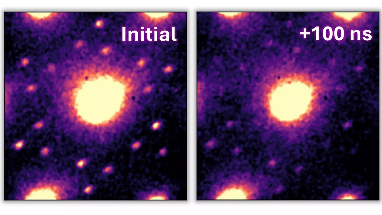
The challenge, however, lies in comprehending the rapidity and intricacy of these waves. Their state shifts occur within minuscule timeframes—often faster than the blink of an eye, making traditional observation techniques difficult. Researchers at the Argonne National Laboratory have tackled this challenge head-on, using state-of-the-art ultrafast electron microscopy to explore the dynamics of these waves, especially within the intriguing material known as tantalum sulfide (1T-TaS2).
A Breakthrough in Observation Techniques
The research led by the Argonne team has yielded remarkable insights into the behavior of CDWs. By applying electrical pulses to 1T-TaS2, they revealed answers to previously cryptic questions about the mechanisms by which electricity interacts with charge density waves. Rather than the anticipated direct influence of the charge current, findings indicated that the heat generated by electrical pulses induces a melting effect in the charge density waves, facilitating significant rearrangements. These results exemplify the unexpected vibratory responses that arise within the material.
This pioneering technique effectively combines nanosecond timing with nanoscale observation, placing scientists at the forefront of understanding electrical switching processes in microelectronic materials. The implications for this knowledge are profound; a deeper understanding of how to manipulate CDWs could revolutionize not just supercomputing but the entire landscape of microelectronic efficiency.
Aiding the Quest for Neuro-inspired Computing
The parallels drawn between the properties of charge density waves and neuronal firing mechanisms underscore an exciting frontier of research. The “melting” mechanism observed resembles neuron activation, possibly ushering in advancements in artificial intelligence and machine learning that are more efficient and closely aligned with biological processes. This neural-network-inspired approach to computing could shift paradigms, moving from our current, cumbersome architectures to systems that resonate with nature’s own designs.
The promise of utilizing materials that can form nanoscale layers, like 1T-TaS2, makes them exceptionally appealing for future microelectronic devices. As the miniaturization of technology persists, being able to harness materials that not only operate quickly but require significantly less power will redefine industry standards.
Broad Impacts Beyond the Lab
While the technical development of these ultrafast electron microscopy methods leads to advancements within specific laboratories, their broader implications can potentially echo through various industries. From consumer electronics to data centers, the thirst for energy-efficient solutions is urgent. Understanding the fundamental mechanisms governing charge density waves can translate to actionable strategies across diverse sectors, driving substantial progress in building sustainable technologies.
Researchers like Charudatta Phatak articulate the broader significance of these findings; the pivotal moment in understanding how to manipulate wave behaviors is just the beginning. As we proceed down this path of innovation, a greener era of computing is not only a hopeful vision but a tangible future within our reach. The journey ahead is certain to be illuminated by the remarkable intersection of physics, materials science, and computer engineering, heralding a new age of efficiency and capability.